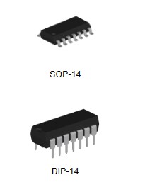
HTC Korea CD4081B consists of four AND gate circuits. Each circuit functions as a two-input AND gate. The outputs are fully buffered for highest noise immunity and pattern
insensitivity to output impedance variations. It operates over a recommended VDD power supply range of 3V to 15V referenced to VSS. Unused inputs must be connected to VDD , VSS, or another input. Unused outputs must be left open.
CD4081B features :
- Wide operating voltage range of 3.0V to 18.0V
- Maximum input current of 1μA at 18V over full package-temperature range, 100nA at 18V and 25°C
- Standardized symmetrical output characteristics
- Noise margin
1.0V min @ 5.0V supply
2.0V min @ 10.0V supply
2.5V min @ 15.0V supply
| Device | Package |
CD4081BD | SOP-14 |
| CD4081BN | DIP-14 |
| ||||||||||||||||||||||||||||||
HTC Korea Logic ICs are designed in South Korea. High quality products, they will match your application needs.

